This is my old idea (and others), to have in-circuit reprogrammable ROM chips in Atari ST machine. Benefits are: easy TOS patching, making some OS additions, and changing TOS version without opening machine or loading TOS in RAM. Now (2008) is ideal time for such upgrade - the prices are very low, so 4 Mbit Flash EPROM costs much less than 1 Mbit (what is size of 1 chip by 2-chip TOS variant) EPROM. And we can have then 4 TOS versions at once, switchable.
The principle: fortunatelly there are some standards (JEDEC), so new ROM chips have practically same pin layout as older ones, except of course new pins (higher addresses). It makes replacement and upgrade relatively simple. Looking standard pin layout by DIL ROM chips used in small computer systems we can notice that GND is always last pin in bottom row - pin 14 by 28-pin chips, pin 16 by 32-pin chips. Data lines are also on same (physical) place, and address lines A0-A14 too. So, we need to care only about pins 1, 2, 30, 31, 32 when replacing 28-pin chip with 32-pin one.
In circuit programming inside Atari ST(E): Flash EPROMs are designed to be programmable inside regular microcomputer architectures, with standard CE, OE, WE signals.
By chips of series 29xxx, 39xxx, 49xxx no need for 12V (as by 28xxx). Reading of Flash EPROMs is exactly same as ordinary EPROMs - need to activate CE, OE while WE is inactive. Of course, all that lines are low-active. In Atari, we need to invert RW signal of CPU, and lead that to OE, RW directly to WE, and to CE connect OR-ed signals ROM0, ROM1, ROM2 - this is at output of 74LS11 (U12 in Mega ST) . Unfortunately it is not enough, because Glue chip will generate bus error by attempt to write in ROM address space. So, we need some additional logic, what will activate DTACK when writing in ROM address space. It is simplest to do with GAL, but may be done with couple logic 74xxx chips.
Boolean equatations are:
/DTACK = /AS*A23*A22*A21*/A20
Above is for TOS 1.6, 2.06... (STE) , address space is $E00000-$E3FFFF .
/DTACK = /AS*A23*A22*A21*A20*A19*A18*/A17*A16 + /AS*A23*A22*A21*A20*A19*A18*A17*/A16 + /AS*A23*A22*A21*A20*A19*A18*/A17*/A16
Later is for TOS 1.00 - 1.04 (ST, Mega ST) . Adress space is: $FC0000-$FEFFFF . Since it is complicated it is best to do with GAL, and then we can solve support for TOS 2.06 by adding address space for it...
Note: DTACK needs OC output for drive. If it is not case, we may connect via schottky diode.
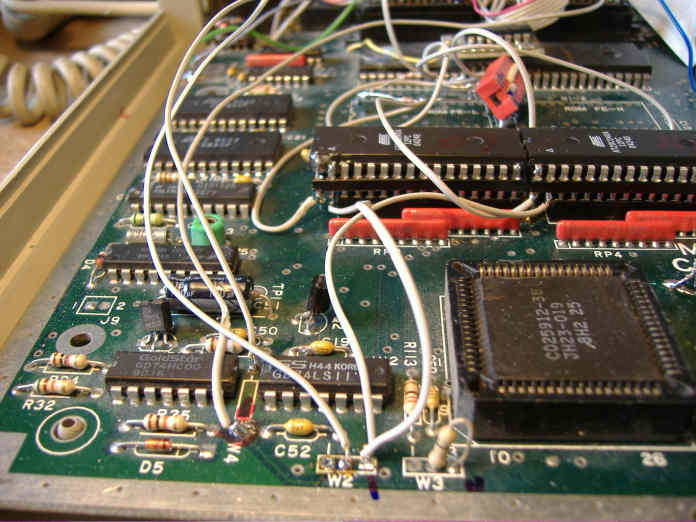
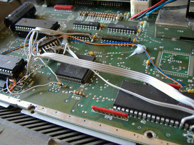
On pic above is how it is solved in Mega ST. 32-pin sockets are inserted in original ROM sockets, so that pins 1, 2, 31, 32 are in air. Pins 30 are cut down, and is best to put little insulator between them and sockets, to avoid contact.
Connectiing of Flash EPROMs: pin 32: +5V (Vcc) , add cer. capacitor between it and GND, with shortest possible legs.
pin 31: (/WE) /RW signal from CPU - via resistor and protection switch (explained later)
pin 30: (A17 of Flash) to selection switch
pin 2: (A16 of Flash) to A17 of CPU - it is closest at W2, point 3 .
pin 1: (A18 of Flash) to selection switch
Other connections in Mega ST: W3 (remains) on pos for 1M ROMs (2-3 connected). W2: remove shortcut and connect point 3 to pins 2 of Flash EPROMs. To point 2 of W2 connect inverted RW signal of CPU (this leads to OE pins of ROMs) .
W4: remove shortcut (if there was 6 chip TOS), Lower point (ROM2 signal) goes to selection logic, upper point comes from selection logic - then need to cut (desolder) pin 12 of 74LS11 , to avoid conflict.
From opposite side:
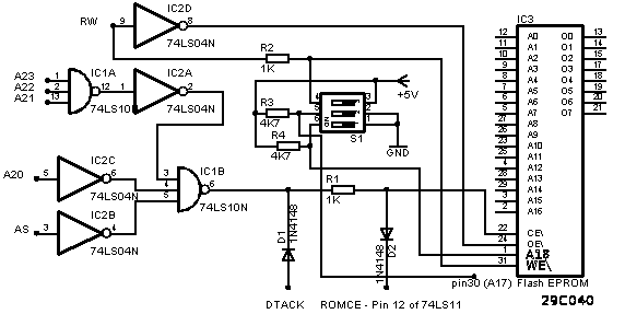
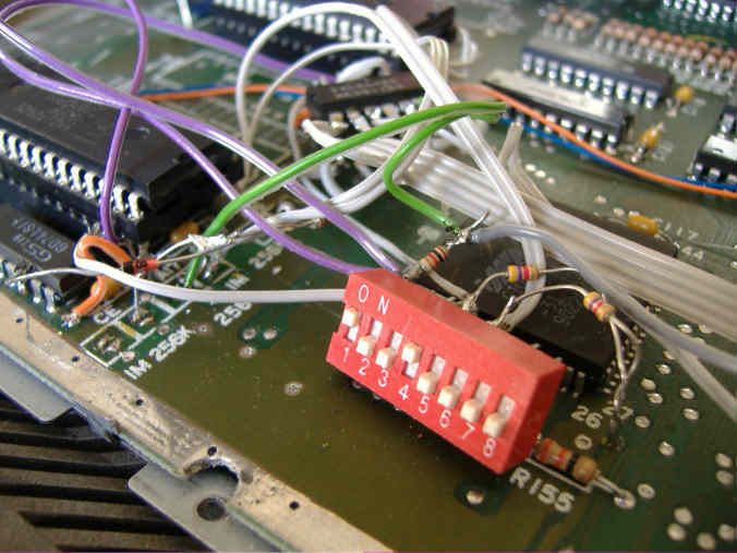
TOS switching: it is very simple. We only change TOP 2 (in case of 4Mbit Flash) address lines states. A17 and A18 of Flash chips. 1 (micro) switch for 1 line. No need for alternate switches: Connect address lines to +5V via resistors of 1K (may vary), and that common point to GND via switch. So, when switch is off it will be on High, and when switch is on, it will be Low.
Protection against accidental writing: again simple solution with switch and resistor - lead RW signal from CPU via resistor of about 470 ohms to pins 31 of Flash EPROMs. Then connect it via third switch to +5V. So, when switch is on, /WE will always be inactive, and no writing happens. When switch is off, it allows write operations.
I did switching with DIP microswitch, where 3 switches are used.
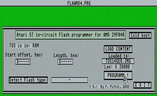
Software for in-circuit programming: I made simple GUI programm for programming Flash inside Atari. There is version for Atmel 29C040 and AMD 29F040 chips. Atmel programs very fast: 256KB (1 TOS space) programs in aprox 5 secs. AMD is little slower because of different (bytewise) programming + required preerasing, but is still very fast: total under 10 seconds for 256KB .
Because TOS and AES constantly accesses ROMs under regular work, we can not do programming with enabled CPU interrupts. Workaround is following: load TOS in RAM (with SELTOS for instance), and then may do programming with GUI SW, and enabled interrupts, since no ROM accessing at all. After successfull programming may click 'Cold boot', for get rid of TOS in RAM. After it usually must press reset button once that machine boot with new content.
Download in-circuit programator for AMD 29F040 with source
1 min video klip of in/circuit programming (3MB, Xvid)
The logic: it can be solved in many ways . Will start with simplest, using GAL chips(s)
Example 1:
% Multi TOS, Supports ROM areas #E00000-#EFFFFF %
% #FC0000-#FEFFFF , writing to Flash EPROMs in area at #E0.... %
% For machines with orig. ROM at #FC0000 %
*IDENTIFICATION
TOSMU1;
*TYPE
GAL16V8;
*PINS
%INPUTS %
A23 = 1,
A22 = 2,
A21 = 3,
A20 = 4,
A19 = 5,
A18 = 6,
A17 = 7,
A16 = 8,
AS = 11,
RW = 12,
ROM2 = 19,
%OUTPUTS %
CER = 18, %E00000-EFFFFF, FC0000-FEFFFF , for TOS 1.xx and 2.06 in same chips%
OE = 16,
DTACK = 17; %connect via Schottky diode to CPU DTACK %
*BOOLEAN-EQUATIONS
/DTACK = /AS*A23*A22*A21*/A20;
/CER = /AS*A23*A22*A21*/A20+/ROM2+
/AS*A23*A22*A21*A20*A19*A18*/A17*A16*RW+
/AS*A23*A22*A21*A20*A19*A18*A17*/A16*RW;
/OE = RW ;
*END
Example 2:
% Multi TOS, IDE . Supports ROM areas #E00000-#EFFFFF %
% #FC0000-#FEFFFF , writing to Flash EPROMs in area at #E0.... %
% For machines with orig. ROM at #FC0000 %
*IDENTIFICATION
TOSMIDE1;
*TYPE
GAL16V8;
*PINS
%INPUTS %
A23 = 1,
A22 = 2,
A21 = 3,
A20 = 4,
A19 = 5,
A18 = 6,
A17 = 7,
A16 = 8,
A5 = 9,
AS = 11,
RW = 12,
ROM2 = 19,
%OUTPUTS %
CER = 18, %E00000-EFFFFF, FC0000-FEFFFF , for TOS 1.xx and 2.06 in same chips%
SELP = 13,
SELS = 14,
IORD = 15,
IOWR = 16,
DTACK = 17; %Goes to inverter with Open Collector e.g. 74LS03 %
*BOOLEAN-EQUATIONS
DTACK = /AS*A23*A22*A21*/A20+
/AS*A23*A22*A21*A20*/A19*/A18*/A17*/A16;
/CER = /AS*A23*A22*A21*/A20+/ROM2+
/AS*A23*A22*A21*A20*A19*A18*/A17*A16*RW+
/AS*A23*A22*A21*A20*A19*A18*A17*/A16*RW;
/SELP = A23*A22*A21*A20*/A19*/A18*/A17*/A16*/A5;
/SELS = A23*A22*A21*A20*/A19*/A18*/A17*/A16*A5;
/IORD = /AS*A23*A22*A21*A20*/A19*/A18*/A17*/A16*RW;
/IOWR = /AS*A23*A22*A21*A20*/A19*/A18*/A17*/A16*/RW;
*END
Example 2 is practically same as 1, but with additional IDE hard disk port control.
But, as we don't have free pins on GAL, we need to invert RW with external inverter, to get /OE signal for Flash EPROMs.
On site is scheme for IDE interface.
IDE IF on expansion slot and switchable TOS with Flash EPROMs in Mega ST.
No GAL programmer? There is a simple solution:
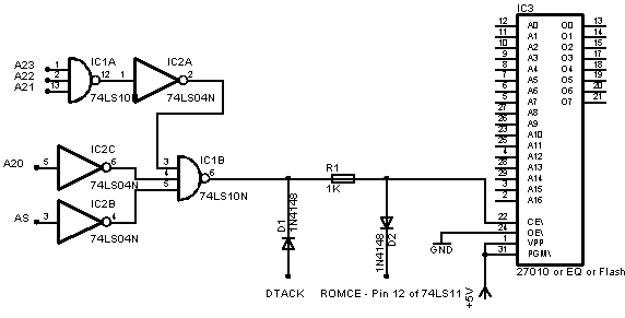
ROM must be connected to GND with pin 14 and to +5V with pin 32 too (power connections) . And 74xxx chips too, of course (pins 7 and 14).
Only 2 cheap IC , 2 diode and 1 resistor required.
In 1040 ST . ROM type selection pads are little different. You need some ohm-meter and pin layout for (Flash) EPROMs to ensure correct pad setting and connections.
Pins 24 of Flash (what are pins 22 of original ROMs) must be connected to GND (short left side of pad marked with A17). From right side of that pad get A17 and connect to A16 pins of EPROMs (pins #2). Pad marked with A16 should be shorted on 1M pos. CE signal from 74LS10, after resistor must go to pins 22 of (Flash) EPROMs, or pins 20 of original sockets - it is connected with pad marked CE, right upper point - disconnect all shortcuts there.
On scheme is read-only version. TOS switch may be added as above - need to may set highest address lines (pins 1 and 30) with some switch to L/H .
For possibility to reprogramm Flash EPROMs just one inventer more is required (there is still 4 free inv. in 2 IC) .
Just couple steps more, and we have reprogrammable TOS:
On scheme is version with place for 4 TOS versions. 2 switch is for TOS version select, third (connected to +5) is for write disabling - to prevent accidental damage of ROM contents. So, open that switch only while reprogramming.
By early 520 ST machines (REV H and earlier) no 74LS11 (and setting pads) - so need to make same 3 input AND logic. May be done with existing ICs, remaining gates: 74LS10 (connect ROM0-ROM2 to 3 inputs) + 74LS04 (as inverter). There are differences by ROM connections on MB too - USB and LSB is used at pins 22, so need to do some wire cuttings too...
Little different pad setting: OE of Flash EPROMs does not connect to GND, but to inverter out. So, no shortcut on left side of pad A17.
Programming SW is same as for "GAL" version. It is not recommended to make reprogrammable version with single-TOS capacity Flash EPROMs. Because, if something goes wrong by programming we will have dead machine after cold boot. By multi TOS switchable we will have always other sections with which can boot machine.
Before starting usage you must program (Flash) EPROMs somehow. Otherwise machine can not be made 'alive' . So, need some programmer device. TOS ROMs must be splitted into High/Low parts, and so burned with programmers .
ROM splitting program with source
It can recalculate and set CRC for TOS 2.06, not only by splitting, but for ordinary binary image files too.
P. Putnik, May, June 2008
Menu Properties Quick Reference
hcnt: 56822